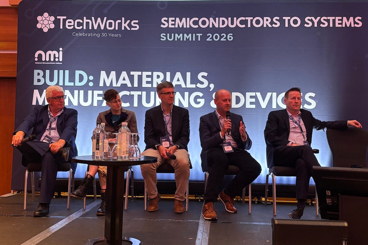
No single semiconductor material can meet every demand of the next generation of power electronics, and engineers across the compound semiconductor industry say that is exactly why the sector is thriving.
Gallium nitride (GaN), silicon carbide (SiC) and a wave of emerging materials each solve a different problem in power switching, from raw voltage handling to blistering fast frequencies. Choosing between them has become an engineering challenge rather than a purely scientific one.
“What a toolbox we have today. You want to switch super fast in power electronics, you go to GaN. You want cheap components, you’ve still got silicon there. You want raw power, you’ve got silicon carbide, and that’s only going to get better as these new materials come down the line,” said Peter Gammon, professor of power electronic devices at the University of Warwick. “Diamond and gallium oxide will continue to offer more and more to that toolbox.”
“It’s a strategic advantage for the UK. If we could do everything with one material, there’s a good chance that would all be done in Taiwan by TSMC (Taiwan Semiconductor Manufacturing Company), and then we wouldn’t be in the game. The breadth gives us the ability to carve out a unique position competitively in the world,” said Jon Heffernan, professor of semiconductors at the University of Sheffield and director of its National Epitaxy Facility.
The National Epitaxy Facility has spent 45 years supplying custom wafers to UK academia and industry.
“If you consider an HVDC (high voltage direct current) brick, in soft switching applications we’re being told silicon carbide is limited to about 600 kilohertz, and in this instance they’re wanting to push to one megahertz. This is where GaN comes into play,” said Daniel Murphy, senior director of product management at Cambridge GaN Devices.
“It’s about the ability to choose which material works best for that application, silicon carbide for high power, gallium nitride for high frequency,” said Katie Hore, innovation director at REWIRE. “It’s not really a physics problem anymore. It’s an engineering problem.”
AI hunts new materials
The comments came during a panel discussion on materials innovation at the Semiconductors to Systems Summit 2026, held in London on August 26 and organized by TechWorks in partnership with the UK Semiconductor Centre (UKSC). The session was moderated by John Lincoln, chief executive of the Photonics Leadership Group.
Venothan Naidoo, head of marketing and business development for the UK and Ireland at Carl Zeiss, and John O’Donnell, global account manager for semiconductor integrated device manufacturers (IDMs) at VAT Group, attended the summit as sponsors.
Roughly 500 distinct semiconductor materials exist, narrowing to about 300 once oxide compounds are excluded, and turning a newly discovered compound into a billion-dollar product has historically taken 20 to 30 years.
Artificial intelligence (AI) is increasingly pitched as a way to speed that up, but Heffernan cautioned it is no shortcut.
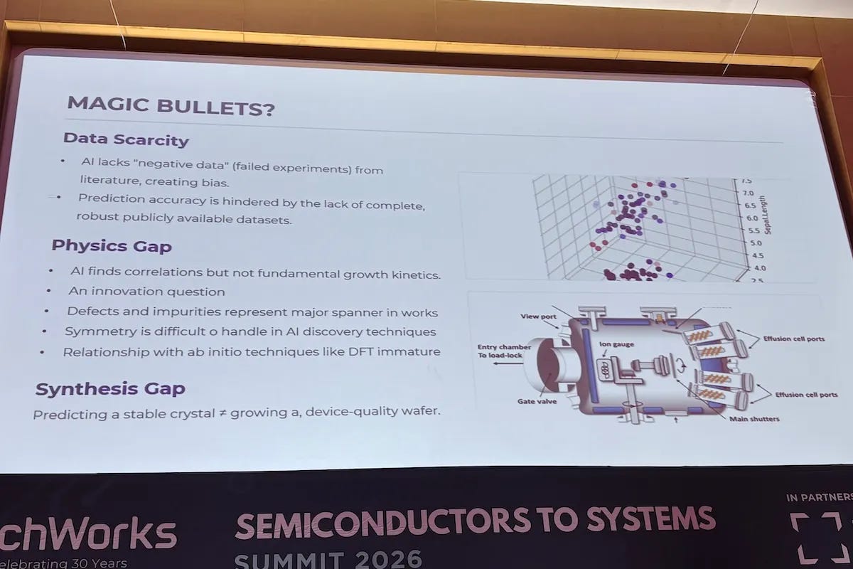
“It’s not as simple as that. The first problem is really data scarcity,” he said. “Large language models (LLMs) scrape the internet and take every piece of information, but for materials discovery there’s a lack of data, particularly negative data. We don’t publish what didn’t work.”
His own slide named two further limits: a physics gap, where AI finds statistical correlations rather than the growth kinetics, defects and crystal symmetry that determine whether a material actually works, and a synthesis gap, where predicting a stable new crystal is not the same as growing a device-quality wafer.
“I can easily grow you very bad quality gallium arsenide. Good quality gallium arsenide is a different ball game,” he said.
Heffernan’s facility, funded by the UK’s Engineering and Physical Sciences Research Council (EPSRC), added a new molecular beam epitaxy (MBE) system last year, and it is now working with AI companies and academics to feed real-time growth data into machine learning models.
That kind of collaboration sits inside a wider push to scale up the UK’s semiconductor base.
Caroline O’Brien, chief executive of CSA Catapult, which is rebranding as the Semiconductor Catapult later this year, told the summit the country already has the ingredients to compete.
“The UK semiconductor opportunity is to turn novel ideas and early-stage technical concepts into industry giants, but we need to do that at scale, and we need to do that at speed,” she said.
She said the number of UK semiconductor companies has grown from 623 in 2024 to more than 700 today, generating an estimated £10.6 billion in revenue in 2026.
“Fundamentally, we need to build the unicorns of tomorrow in the UK. Our ‘North Stars’ (guiding strategic goals) at the Catapult are basically AI hardware and defense, and as we become the Semiconductor Catapult later this year, we want to converge the technologies we have across the supply chain: power, radio frequency, photonics and advanced packaging," she said.
From lab to fab
Murphy said Cambridge GaN Devices, a spinout founded by Giorgia Longobardi, who studied for her doctorate at the University of Cambridge, together with power semiconductor specialist Florin Udrea, has built its business on packing more circuitry directly onto the chip.
“We’re at a point now where we have approximately 80 patents on gallium nitride,” he said, noting that Infineon, a company of roughly 50,000 people, paid more than $800 million to acquire GaN Systems, which holds about 400 gallium nitride patents. “For 70 people to produce that many patents is very good going.”
Cambridge GaN Devices’ own count puts the precise total at 77 granted patents and more than 146 pending applications, held by a team of 70 across sites in Cambridge, North America, Shenzhen and Taipei.
“By integrating a circuit onto the GaN, you’re simplifying the external components and the bill of materials around the system. You’re reducing the component count, you’re reducing the area of the board,” he said.
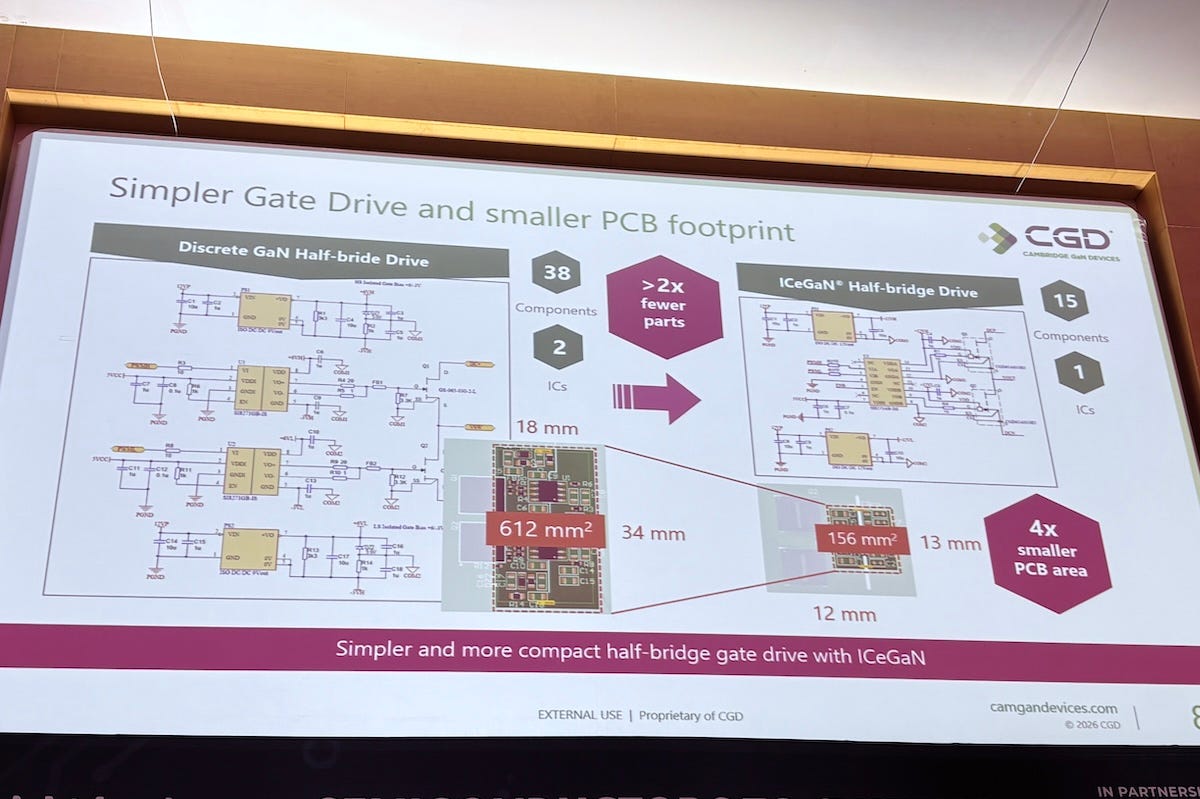
The company’s own comparison shows a conventional half-bridge gate drive needing 38 components across 612 square millimeters of board space, against just 15 components in 156 square millimeters for its ICeGaN platform, more than four times smaller.
He said the company’s parallel-connected devices delivered a clean 140 amps in testing. Independent trials at Virginia Tech showed its transistors withstand gate voltages of up to 80 volts, well above the 20 to 30 volts at which conventional gallium nitride transistors typically fail.
REWIRE, the £11 million UKRI (UK Research and Innovation) funded innovation and knowledge center where Hore and Gammon work, is chasing similar gains in silicon carbide.
“Today, we’ve managed to double the industry metric of mobility in that area. We’ve managed to halve the resistance that’s being associated with that interface,” he said.
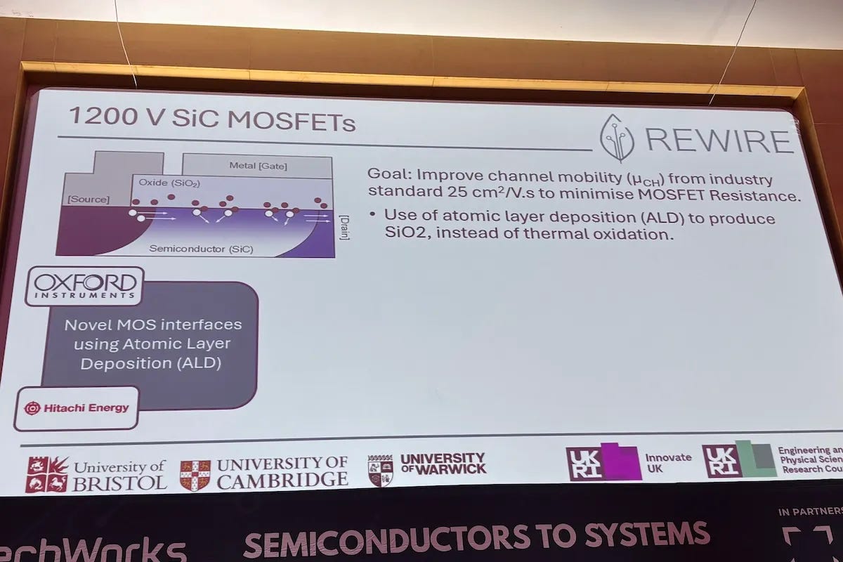
REWIRE’s own figures put the industry-standard channel mobility it is improving on at around 25 square centimeters per volt-second, achieved with atomic layer deposition (ALD) rather than conventional thermal oxidation.
He said the work has moved from 1,200-volt devices to 2,300 volts through a REWIRE flexible funding project with Clas-SiC Wafer Fab, and a separate flexible funding project is helping UK startup KuasaSemi optimize its TCAD (technology computer-aided design) chip design software.
Iwan Davies, group technology director at IQE, which has grown compound semiconductor materials for 38 years from its Cardiff headquarters, said the company’s own scale-up work shows how far the field still has to go.
“This is an example of a 200 millimeter VCSEL (vertical cavity surface emitting laser) wafer, which we announced in 2022. You see a photograph there of a 200 millimeter VCSEL, which has a quarter of a million devices,” he said.
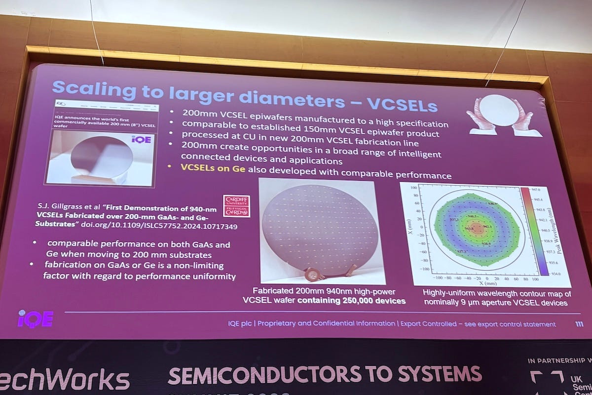
IQE said the wafer, announced in 2022 and processed through a pilot line at Cardiff University, contains exactly 250,000 devices.
“This is working with Lancaster University and its spinout Quinas on memory devices, an indium arsenide aluminum antimonide triple barrier device for a universal memory application, for things like neuromorphic computing, AI and so on,” he said.
The project, known as ULTRARAM, combines the non-volatility of flash memory with the speed of dynamic random access memory (DRAM). IQE and Quinas Technology completed a £1.1 million industrialization project on it, targeting AI, neuromorphic computing and space and defense applications.
He said the CSconnected cluster project, which concluded on August 31 after six years, was worth around £43 million, mostly for collaborative research and development.
IQE’s own figures put the precise total at £43.7 million.
REWIRE, IQE and Cambridge GaN Devices are all pushing their materials from campus labs toward production lines, and the panel’s shared message was that the UK’s advantage lies less in picking a single winning material than in mastering many of them.