


For decades, chipmakers picked an application and then hunted for a material that could deliver it. That order has quietly flipped. A growing number of companies now start with the application and design an entirely new material to fit it.
The clearest evidence sits at the atomic scale, where materials just one atom thick behave nothing like their bulk counterparts.
“So many AI (artificial intelligence) companies have come to me over the past few years saying, ‘Which application do you want? Let us design the material for you,’” said Dr. Simon Thomas, chief executive of Paragraf. “It is the lead of what we’re trying to do.”
“It’s been wonderful seeing the results you can get in the lab,” Thomas said, “but that doesn’t mean anything to the real world unless you can get it to industrial scale and convince people they want to use the material.”
That is the gap Paragraf has spent years trying to close.
Named for graphene, the world’s first two-dimensional material, discovered in Manchester, the company built its own UK foundry to turn lab demonstrations into products, including sensors that use 1,000 times less power than conventional alternatives.
Graphene is only the start of the family, which includes transition-metal dichalcogenides, boron nitride and emerging oxides called MXenes (two-dimensional metal carbides). He said stacked materials can form structures that bulk materials simply cannot support. The obstacle is not the material itself but the join between them.
“The problem is when you start to use 2D materials that are not epitaxial, you start to get electrostatic problems,” Thomas said. “The interface of 2D materials, when you put them together, is the real challenge right now.”
He said the industry solved similar problems before while combining materials for laser diodes and LEDs. Major chip foundries already have big ambitions for 2D materials.
John Tingay, chief technology officer of Oxford Instruments Plasma Technology, backed the assessment from elsewhere on the panel.
“We’ve got this very strong 2D materials [community], both from academia and from Paragraf, a big head start in that space,” he said.
Paragraf’s own roadmap points to where that head start could lead.
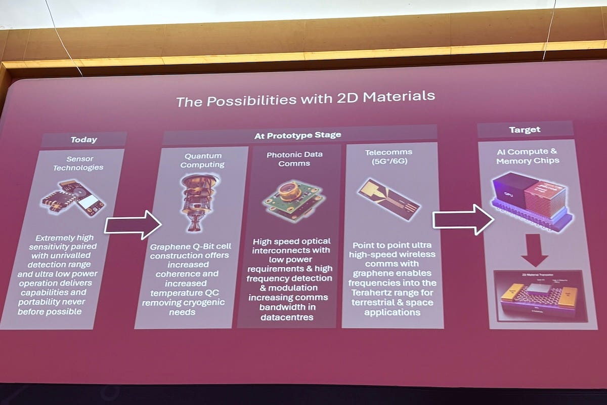
Sensor technologies are already on the market; quantum computing and photonic data comms are at the prototype stage; and the eventual target is AI compute and memory chips.
With silicon's transistors nearing the atomic-scale limits that mark the end of Moore's Law, Thomas said the industry has little choice but to engage with the shift.
“Why not use the ones that are fit for purpose, instead of just trying to make silicon smaller and smaller?” he said.
Moore’s Law is the 1965 observation by Intel co-founder Gordon Moore that the number of transistors on a chip roughly doubles every two years. It is fading because, at just one or two nanometers, transistors are so small that electrons leak through the gate via quantum tunneling, sapping efficiency and generating heat.
Betting big on scale
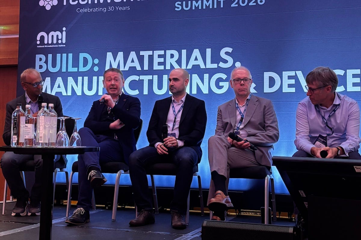
The presentations were part of the Semiconductors to Systems Summit 2026, organized by TechWorks with the UK Semiconductor Centre on August 26. Nitin Dahad of EE Times moderated the session on turning new materials into manufacturable processes.
Two of the speakers are already running high-volume UK production lines built around difficult materials of their own. Ian Croston, vice president of operations at Lumentum, said the industry’s real bottleneck has little to do with graphics processing units, and everything to do with something more basic.
“Inside every data center there is a connection problem, and that connection problem is copper. Copper cables and connections cannot keep up with the data rates now being routed through data centers, and the answer is fiber optics,” he said.
Lumentum’s UK site in Caswell, Northamptonshire, sits at the center of its expansion to meet that demand.
“We are increasing our manufacturing capacity over the next two years by more than tenfold, and we’re expanding our workforce by about 30% to 40%,” Croston said.
Caswell traces its semiconductor roots back more than 70 years.
The site produced some of the UK’s earliest gallium arsenide monolithic microwave integrated circuits (MMICs) and indium phosphide lasers starting in the 1970s, and now covers the full value chain, from epitaxial growth through to finished devices, with around 350 people on site.
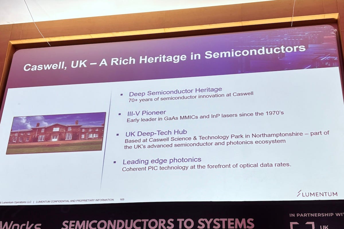
Its photonic integrated circuits (PICs) are used in long-haul terrestrial and submarine networks.
“There are only two primary suppliers of these PICs on the planet, ourselves and Coherent, so it’s quite likely you’ll use one of our devices,” Croston said. “At completion in 2028, we will probably be the largest photonics indium phosphide fab, not only in the UK but in the rest of Europe.”
Dr. Feras Alkhalil, vice president of research and development at Pragmatic Semiconductor, is chasing a different kind of scale from the company’s own 300-millimeter line in Durham, and said Pragmatic is not trying to replace silicon everywhere.
“We’re introducing a differentiator for applications where we believe we can displace silicon in those use cases,” Alkhalil said.
Pragmatic closed a Series D funding round of more than £182 million at the end of 2023, the largest European venture round of its kind at the time, backed by investors including M&G and the UK National Wealth Fund.
“Pragmatic Park, our manufacturing facility in Durham, is currently the only 300-millimeter manufacturing facility in the UK,” Alkhalil said.
“We have two 300-millimeter lines there now, and capacity for up to nine lines going forward,” he said. The facility is designed to scale toward the trillions of units he expects wider adoption will require.
“These are low-carbon solutions compared with conventional technology,” Alkhalil said. “They consume much less energy, water and chemicals.”
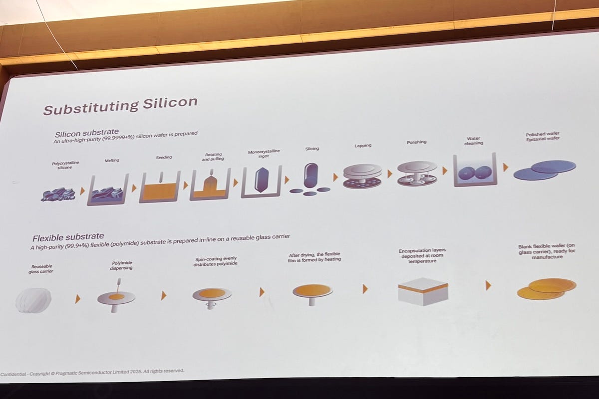
He said a traditional silicon wafer starts as an ultra-pure ingot, melted, pulled and sliced at high temperatures, while Pragmatic’s flexible substrate skips that step entirely, built up instead on a reusable glass carrier that can be used again and again, then coated, dried and encapsulated at room temperature.
“We’re bringing radio frequency identification (RFID) and near-field communication (NFC) products to our customers this year,” Alkhalil said. “Part of that same product family is also designed to stop physical counterfeiting.”
Running short on people
Not every constraint on that ambition is technical. Croston said the industry’s growth is limited less by manufacturing capacity than by people.
“Do we have the right people, and are there enough of them? The answer is no, and no,” he said.
“The UK does not value people, doesn’t value talent, doesn’t value how we can get talent moving very quickly,” Thomas said, adding that the visa system makes it hard to bring in overseas specialists who could train staff inside British companies.
“If we’re really serious about having talent in this country, we need to do the short-term thing, which is educate people now in the workplace, and the long-term thing, which is commit money to STEM (science, technology, engineering and math) subjects targeted at industry,” he said.
Croston said companies have their own work to do too.
“It isn’t just about the money or the package, although that’s important,” he said. “It’s about making the site a pleasant place to work, and about whether I can grow my career at this company.”
Alkhalil said the answer has to run through schools as much as companies.
“Industry has a role to play. We have lots of apprentices, we bring in schools and colleges, and universities and academia have a role too,” he said.
The panel traced much of that shortfall back to a lack of national direction.
Thomas said the UK cannot compete with chipmaking giants on scale, so success depends on picking a lane and figuring out how to grow the seat at the table it already has.
“We’re never going to be like TSMC, but we do innovate better than most places in the world. I don’t think anyone in the manufacturing world understands what the government really wants right now, and stability for business is critical, absolutely critical,” he said.
Tingay placed the problem in a global context. He warned that efficiency gains alone will not solve the industry’s power problem.
“This same conversation is happening everywhere. If you can’t play in silicon, if you don’t have a TSMC, an Intel or a Samsung, you’ve got to find something else to do,” he said. “You’d only need a 1% improvement in power distribution within data centers to save enough energy to power an entire major city.”
He recalled the 19th-century economist William Stanley Jevons, who found that more efficient steam engines did not curb coal use as engineers had hoped. Instead, cheaper running costs led people to build and run more of them, a dynamic now known as the Jevons paradox.
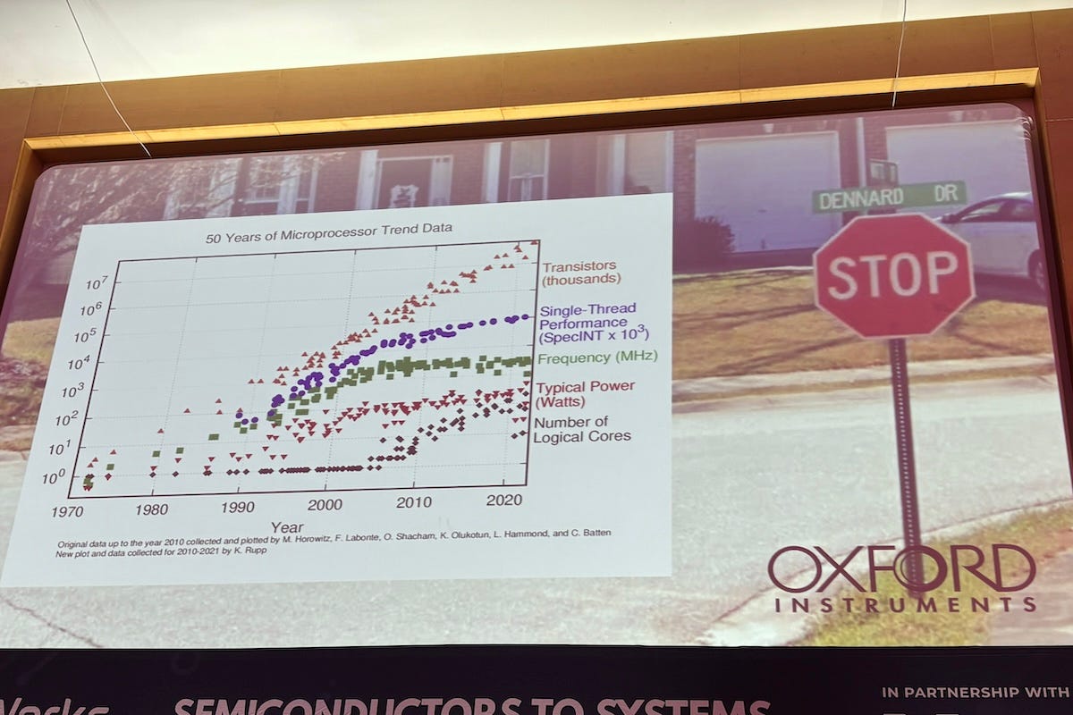
“Small changes just get used up,” Tingay said. “You have to make substantial changes to get any benefit. The real improvements come from fundamental device and material changes, the same kind of thing Paragraf and Pragmatic are doing with whole new structures.”
Between Lumentum’s push to become Europe’s largest indium phosphide fab by 2028 and Pragmatic’s climb toward trillions of low-carbon chips a year, the UK’s near-term test will be whether its manufacturing ambitions can outpace its persistent shortage of skilled engineers and technicians.