Semiconductor engineers are supposed to spend their days making sense of data, tracing the patterns that reveal why a wafer failed or a process drifted, not stuck on the mechanical work of capturing it in the first place.
In a typical metrology workflow, sample preparation and data capture can consume 70% to 90% of an inspection’s time, leaving less than 10% for the analysis that actually informs production decisions.
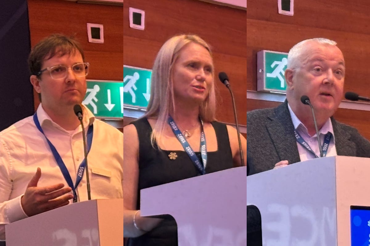
“The operators on the ground should be spending more time on the useful component, analyzing the data, rather than capturing it,” said Andrew Elliott, business development lead at Carl Zeiss Ltd. “You want the data capture stage to be as small as possible.”
Carl Zeiss Ltd is the British arm of the German optics and instruments group. It supplies inspection tools ranging from basic light microscopes to high-end scanning electron microscopes, with resolutions ranging from roughly 700 nanometers to under 1 nanometer, covering routine wafer checks up to atomic-scale imaging.
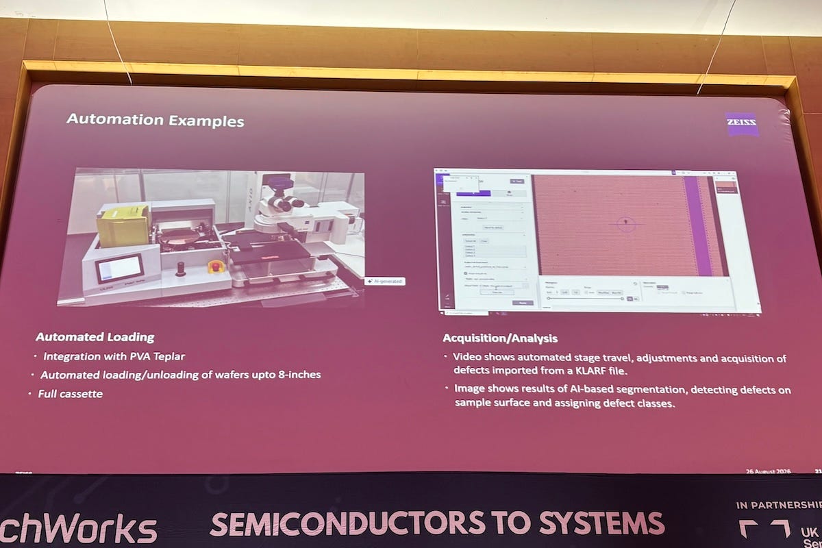
One example is the Zeiss AxioImager Vario, a light microscope adapted for automated defect review. The system uses PVA TePla technology for automated wafer loading, then software that navigates to defect coordinates supplied by a KLARF file from a KLA inspection tool.
“All the user has to do is essentially press go at the start, and that will capture all the data for them,” Elliott said.
Once captured, the images are automatically segmented and color-coded so a human operator can interpret them quickly.
He said that cuts the time spent on quality control and quality assurance checks, letting more wafers move through per hour.
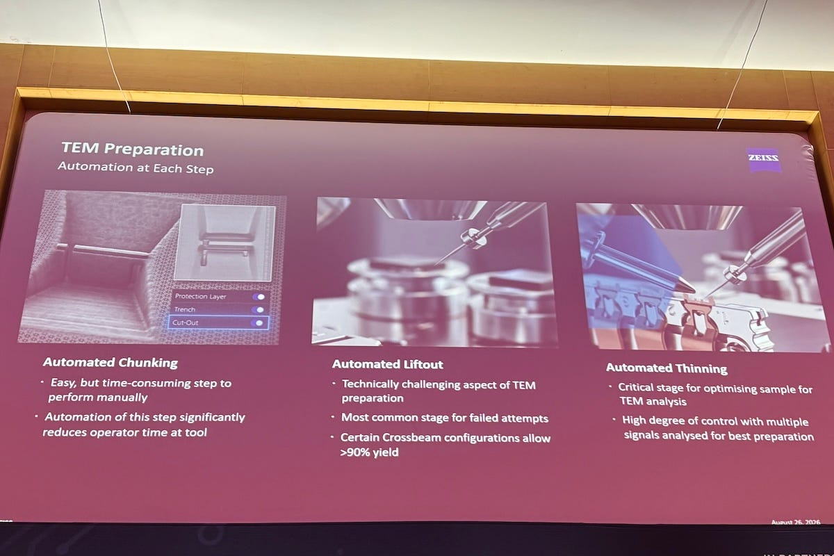
A similar principle applies to preparing samples for transmission electron microscopy, a technique that requires shaving a wafer sample down to tens of microns across and under 100 nanometers thin. Preparation traditionally runs on a focused ion beam scanning electron microscope and can take an operator an hour or more per sample.
Zeiss has automated all three stages of that process, chunking, liftout and thinning, on its Crossbeam 750 system. Automating the chunking stage alone frees up 30 to 40 minutes per sample, the biggest single time saving in the workflow.
Lift-out is not the longest of the three stages, but it is historically where most samples are lost.
Elliott said that automating lift-out now delivers yields above 90% for this technically demanding step, while automated thinning uses an array of detectors to stop each sample at the precise thickness required for a clean image.
He said Zeiss is extending automation across its broader portfolio, including X-ray microscopy, contact measurement tools, and other scanning electron microscopes, and stressed that the goal is not to eliminate jobs but to rebalance the time operators spend capturing data versus analyzing it for decision-making.
“It’s changing the amount of time an operator is spending doing the capture compared to how much they’re spending doing the useful stuff with the useful data,” he said.
Detective work still needed
Elliott’s presentation was part of the Semiconductors to Systems Summit 2026, held in London on August 26 and organized by TechWorks in partnership with the UK Semiconductor Centre. The session on intelligent and reliable manufacturing was moderated by Steve Reynolds, strategic business development manager at the National Physical Laboratory (NPL).
Suzanne Costello, founder and chief executive of Forensic Eyes Ltd, said artificial intelligence (AI) can flag semiconductor defects but cannot always explain what caused them, and her company investigates failures across the electronics supply chain, from printed circuit boards to fully packaged devices, spanning consumer, medical, aerospace, defense and automotive products.
Costello opened with an image of a semiconductor device showing unexplained lumps on a dielectric layer and asked the room what had caused them, a reminder that spotting a defect is only the first step toward understanding it.
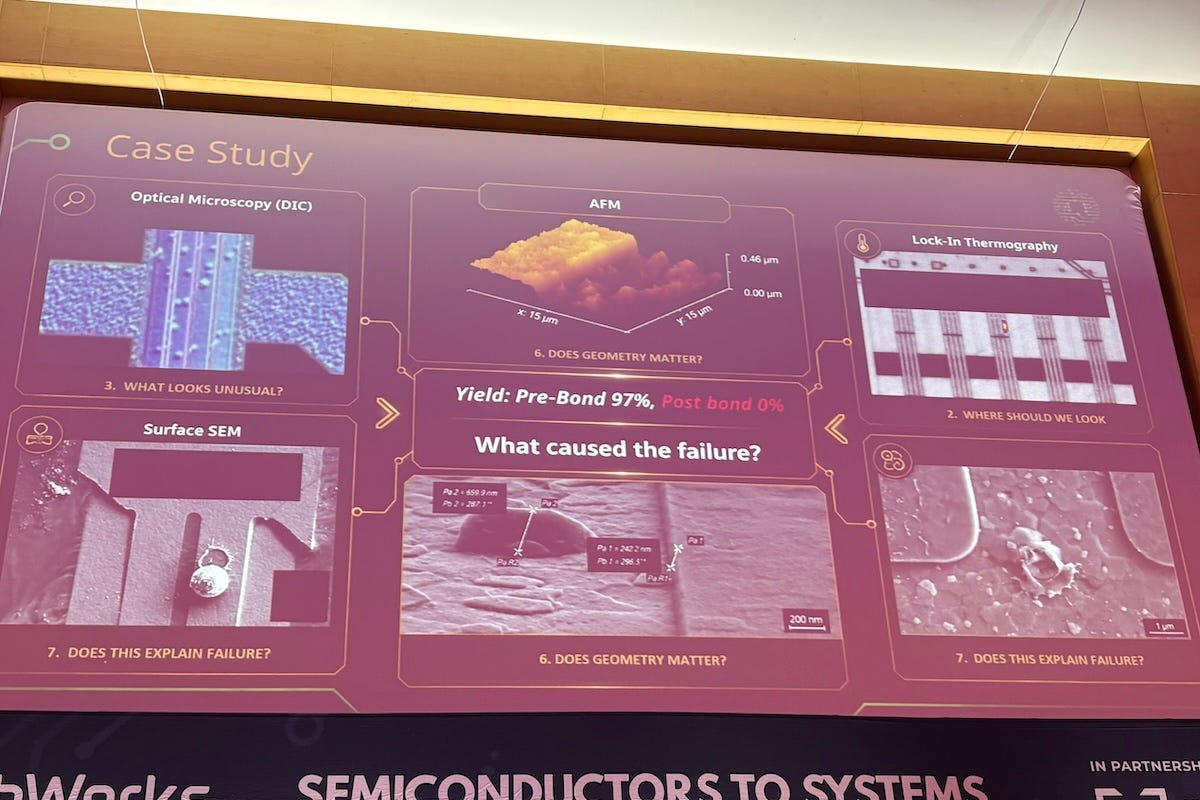
She said nobody in the room could explain it immediately, not even her own team.
“AI is really good at process. If you were looking to code something, let it run through; it will take you all the way through that process. However, if you’re looking to solve a problem, you need to know that the time you’re spending will produce the results you want. That’s where humans come in,” Costello said.
She said engineers bring critical thinking and judgment that still require direct interaction with the customer. She illustrated the point with a live case study involving a microelectromechanical systems (MEMS) device in late-stage development. Pre-bond yield stood at 97.24%, but yield collapsed to zero immediately after bonding.
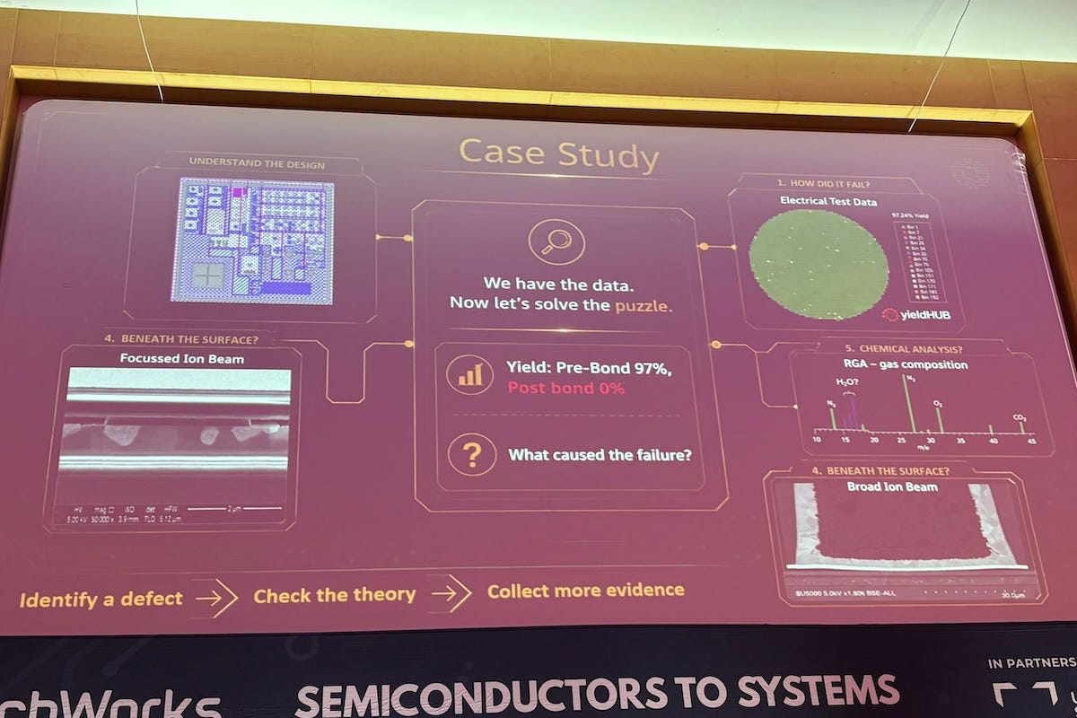
Costello’s team initially suspected a packaging failure and used focused ion beam analysis to examine bridges that had visibly flattened and stuck to the surface. Residual gas analysis then ruled out moisture as the cause, since the package remained properly sealed, sending investigators back to the sample for a second look.
Closer inspection revealed metallization lumps near the dielectric’s height; atomic force microscopy confirmed hillocking; and thermography pinpointed a short circuit.
A second group of failed units showed no hillocking at all, pointing instead to contamination on the underside of the bridges once they were removed and inspected.
“We’ve actually got at least two mechanisms giving one failure mode,” she said.
The team traced both mechanisms through the customer’s process and proposed a design change that let production continue on a well-yielding device while a longer-term fix was developed. She said that as long as engineers keep working with new materials, there will always be a need for humans who understand how they interact.
She also used her slot to introduce FAXTYR, a TechWorks steering group. Its name stands for Failure Analysis, Characterization, Test, Yield and Reliability.
The group’s first task is to map failure-analysis capability, equipment, and resources across the UK, then use the results to identify gaps and lobby government and industry to close them, both to support sovereign chipmakers and to attract overseas investment.
Turning data into savings
At the same event, John Moylan, operations senior manager at Vishay Newport Limited, said the company runs the largest single semiconductor manufacturing site in the UK.
He said Vishay Newport has built its operations around a manufacturing execution system called PROMIS, which feeds finance, capacity planning, scrap reporting and dispatch systems, giving the company standardized execution, full traceability and real-time decision-making across a factory that runs 24 hours a day, every day of the year.
“Fact- and data-driven decision-making is fundamental to us,” Moylan said, adding that the approach has driven high throughput, lower variability and reduced manual intervention on the factory floor.
He said the data-driven culture has generated more than $4.9 million in savings opportunities across the site.
A quality-improvement circle used lot-level and process-level scrap data to drive the weekly scrap rate on its SP10K final test line down toward zero, saving $42,000 in a single year, while a separate push against repel errors saved a further $17,000 in 2025.
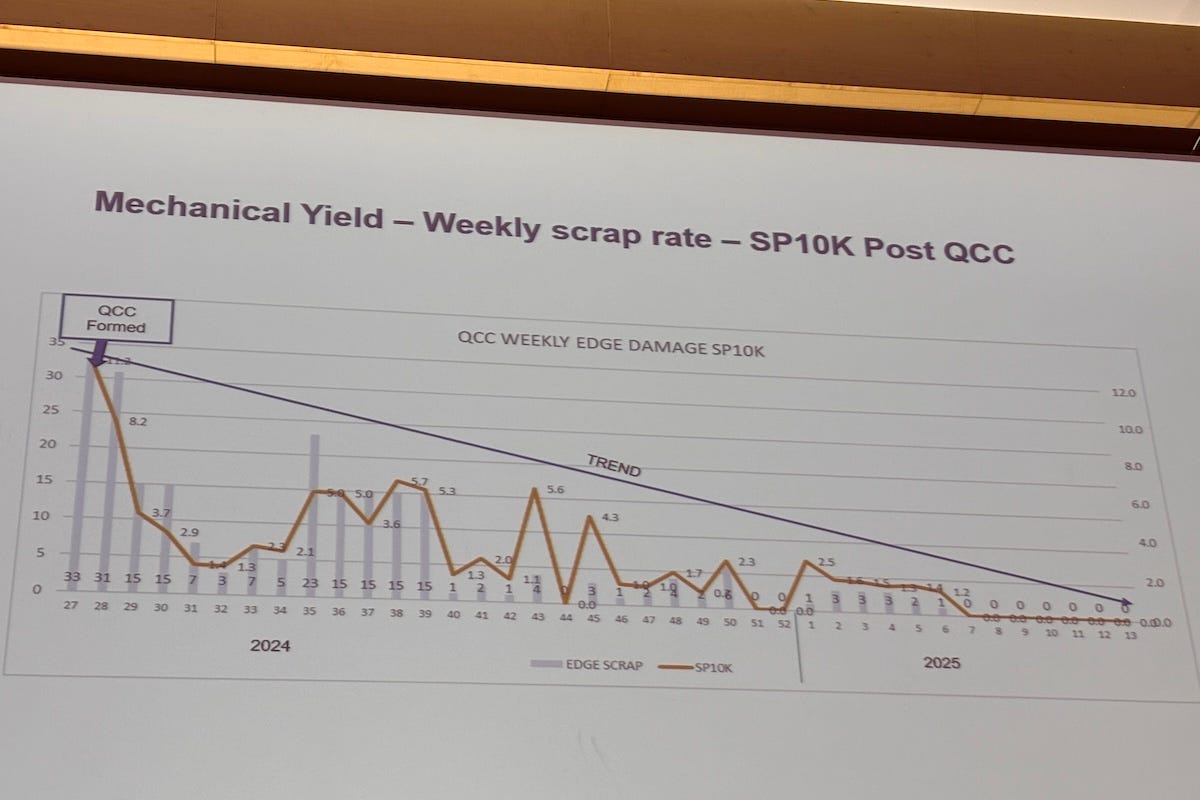
The company’s 3D printing department, drawing on the same tool-level data, is on track to save $513,283. Process improvements elsewhere across the site have already returned 2,539 productivity hours.
Moylan said engineers can now redirect that time toward root-cause analysis and higher-value work. He said the savings extend beyond the balance sheet, pointing to Vishay Newport’s roughly 2% absence rate.
He credited that to strong employee retention, built on continuous investment in people and processes rather than on headcount growth. He said that culture is reinforced by promoting from within.
The company has spent several years developing talent internally, moving former operators into technical support, leadership, engineering and module manager roles, until continuous improvement becomes not just part of the job at Vishay Newport but the job itself.
Vishay Newport has been a member of the National Microelectronics Institute (NMI) for more than 25 years and hosted three NMI events in 2026 alone.
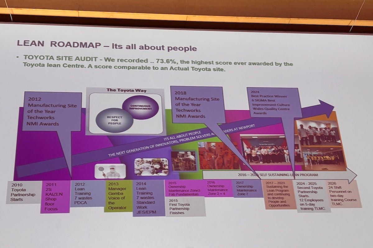
The company also has a long-running training partnership with Toyota’s plant in Deeside, North Wales, sending staff there regularly and hosting Toyota auditors on site. Earlier this year, it also hosted a Welsh Government event that brought Toyota and other regional manufacturing leaders onto its site.
That partnership underpinned back-to-back Manufacturing Site of the Year wins at the TechWorks NMI Awards in 2012 and 2018, a Best Practice award from the Wales Quality Centre in 2024, and a 73.6% score in its most recent Toyota audit.
Moylan said Vishay Newport's next priorities are deeper automation, more advanced analytics and faster decision-making, extending the PROMIS-driven approach that has already delivered millions of dollars in savings and stronger retention across the site.