


The custom chips powering the artificial intelligence (AI) boom are outgrowing the design methods engineers have relied on for decades.
Single dies are out of room, so designers stitch many into packages that bend, warp and trap heat.
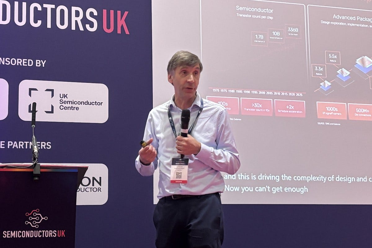
“If you look at a typical AI accelerator today, it is a massively complex chip. It’s generally manufactured to the biggest possible size and has a huge number of AI accelerator components, and this is driving the complexity of design,” said Rod Metcalfe, senior group director in the Digital Design Group at Cadence.
“Now you can’t get enough transistors on a single piece of silicon anymore,” he said. “So the next thing is packaging. We’re pushing the limits of packaging all the time.”
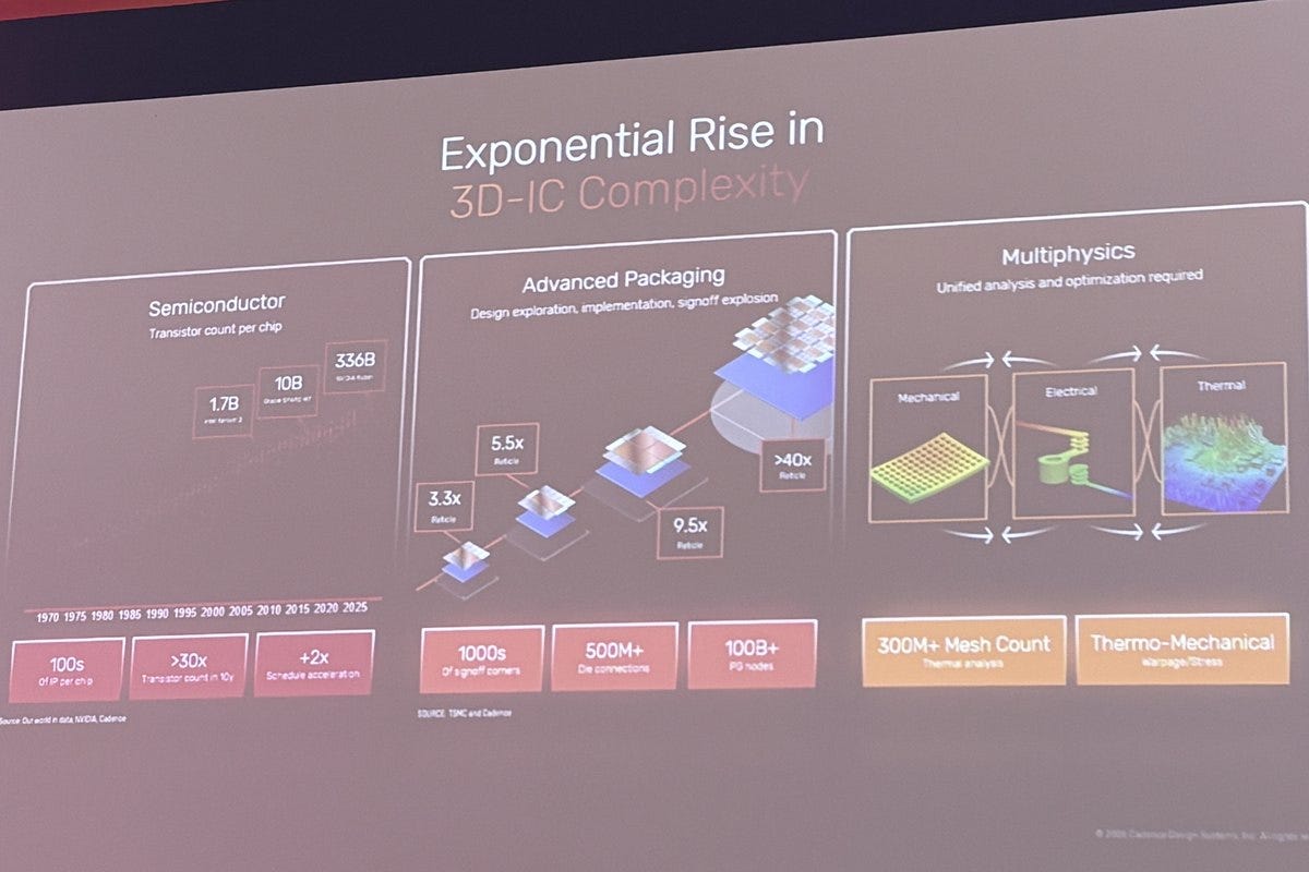
Advanced packages have grown from 3.3 times the reticle limit, the largest area a lithography tool can print in one exposure, to more than 40 times. Transistor counts per chip have risen more than 30-fold in a decade, while design schedules have had to move twice as fast.
Signing off such a package means checking thousands of operating scenarios, more than 500 million die connections and over 100 billion power-grid nodes. Thermal analysis alone can involve more than 300 million mesh elements.
Metcalfe said putting many dies in one package makes mechanical stress and heat major design problems.
“If you’ve got a giant package, it’s going to bend and warp. Thermal is a huge problem. You can put lots of pieces of silicon in a package, but if you can’t get the heat out, they’re not going to go very fast,” he said.
Demand is not in doubt. IDC forecast in February that global semiconductor revenue would reach $1 trillion this year and $1.4 trillion by 2030. Bank of America raised its 2026 estimate to $1.3 trillion in April.
“It’s great to have growth in the industry, but we need some ways of resolving this increasing complexity, the additional packaging constraints and all the analysis, like thermal and physical effects, that come along with that. If we’re going to scale chip design, we need to do it a lot faster,” Metcalfe said.
Cadence, a California-based supplier of electronic design automation (EDA) software, launched a series of AI “super agents” this year, each running a whole stage of the design flow, from verification to digital layout and packaging.
Forty years of abstraction
The keynote, on deploying AI super agents to accelerate chip design, was given at Semiconductors UK, part of the Microelectronics UK 2026 conference organized by IQPC Exhibitions in London on September 29. Conference chair Martin McHugh, board chair of Novomorphic, introduced the session.
Metcalfe has worked on machine learning tools for chip implementation at Cadence since 2015.
“Everybody thinks AI is the first change in chip design. That’s absolutely not true. For people as old as I am, we may remember people designing transistors individually. That took a very long time,” he said.
Engineers later grouped transistors into standard cells, then used register-transfer level (RTL) synthesis to generate the netlists that connect them. Specifications can now be written in high-level C (a programming language) and compiled automatically. Each step raised the level of abstraction, backed by ever more capable solvers for tasks such as placement and routing.
“Over the past 40 years, we have been increasing productivity through abstraction. AI technology is just the next evolution of this. We can take the abstraction level even higher,” Metcalfe said.
He said AI can now generate RTL straight from a design specification, but language models will not replace solvers.
“Large language models (LLMs) are not good at doing everything. If you want to do the final placement of a 5 million cell design, it is very inefficient to do it through an LLM. It’s much better to use a solver,” he said.
AI in chip design now comes in three levels:
Optimization AI built into solver engines, which predicts outcomes to cut runtime
Tool agents that turn high-level prompts into scripts
Super agents that orchestrate a sequence of tools across a whole workflow
Today’s EDA tools are single programs driven by scripts. A super agent instead pulls in documentation, design data and several tools to decide its next step. Engineers deal with it at a much higher level, describing the job rather than scripting each tool.
“You describe the task you want it to perform, and then the agentic system will gather the information and generate a result. This is very different to a single program that performs a task,” Metcalfe said.
Retrieval-augmented generation (RAG) pipelines feed tool documentation into a knowledge source that the agent consults before acting. Where a traditional EDA tool runs on millions of lines of C++, a super agent is built on millions of lines of Python scaffolding and natural-language skills.
Locking down design data
Letting agents roam freely poses a security risk for chipmakers, whose designs are among their most valuable intellectual property.
“What you don’t want is all these agents going off and connecting to the internet and trying to do something, because before you know it, all your design data is on the internet,” he said.
Metcalfe said all agents should reach language models through a single controlled gateway. That could mean commercial models such as ChatGPT, Gemini and Claude, or models running on a company’s own graphics processing unit (GPU) cluster, which he called the most secure option.
In a live demonstration, an agent ran a digital implementation flow on its own, building the flow before running it.
It hit a problem during synthesis and fixed it, then found congestion in the floor plan that would have stopped the design from completing. It cleared the congestion, rebuilt the floor plan and ran placement again. Each loop back marks a fresh iteration of the flow.
“The agent is managing not only doing the design but correcting it as we go through the flow. While one agent’s doing one thing, another agent can start optimizing a different design,” Metcalfe said.
A second agent cut the power consumption of another block in parallel.
Autonomous runs on blocks of 5 million to 6 million cells can take several days, so engineers can also work with agents interactively, for example to debug a design, handle floor planning or improve one particular area.
He said agents can also design three-dimensional integrated circuits (3D-ICs), placing cells across stacked logic tiers that each become a separate chip. Slicing a typical central processing unit (CPU) design into several chips this way improves power consumption, wire length and performance.
“What we see here is the ability to design a single chip across multiple dies, and this is a very good way of allowing you to grow the design beyond the size of one chip,” he said.
Metcalfe said some of the technology he showed is still in development, as designers look to agents to help assemble memory and logic dies into single 3D packages, a task that grows harder as AI chips outgrow the limits of a single die.