


Britain has no domestic source of interposers, the high-density wiring layers that link chips inside advanced packages, so developers must buy them abroad.
Interposers made of silicon or glass already sit inside phones and high-end processors, carrying signals between chips through fine copper tracks and vertical channels called vias. The finest versions come from large foundries in Europe, Asia and the US, built with heavy investment.
“If you want that kind of fine pitch, single-digit micron through-substrate via, you can go to Europe, Asia and America and get that. But you can’t get that indigenously in the UK,” said Sean Butterworth, lead technologist at BAE Systems.
“In an early phase, you may only need to make 10 pieces. But you need to buy 10,000 at great expense,” he said. “There’s no supply chain in the UK which can offer small-volume production for defense or civil applications when people are prototyping.”
BAE Systems, a British defense and aerospace group with more than 110,000 employees in over 40 countries, builds fighter jets, submarines and aircraft carriers. Butterworth works in its air business, which makes the Royal Air Force’s Eurofighter Typhoons.
Tier-one chipmakers already use interposers in high-end processors, including Intel’s Panther Lake laptop chips unveiled in October 2025.
A consortium led by BAE Systems is now building a UK alternative, aimed at small batches rather than the volumes tier-one foundries serve.
“We will not be competing with those tier-ones who do ultra-fine pitch because they’ve had billions of dollars’ worth of investment into their foundries, which we don’t have in the UK,” Butterworth said. “If you want lots of high volume, you’ll go abroad.”
The group is targeting niche, low-volume work with a highly customizable process design kit (PDK), the set of design rules customers follow. It accepts off-the-shelf dies and chiplets and fits with existing UK packaging houses, some of which already package chips on interposers supplied by customers.
Its baseline offering is 40-micron-diameter vias through a 300-micron-thick wafer, which his slides describe as widely considered a step change over printed circuit board (PCB) technology without needing tier-one facilities.
“Our offering at the moment is quite modest. These targets were set because this was based on Innovate UK work, and you have to set a goal that’s achievable,” he said.
Tracks 30 times finer
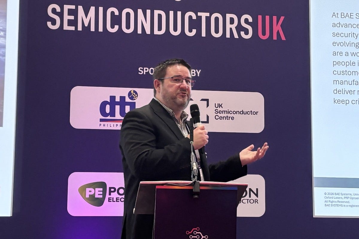
The BAE Systems engineer spoke at Semiconductors UK, part of the Microelectronics UK 2026 conference organized by IQPC Exhibitions in London on September 29. Conference chair Martin McHugh, board chair of Novomorphic, hosted the questions that followed his talk on building a sovereign UK interposer supply chain.
Butterworth holds a PhD from the University of Manchester and moved from university spinouts into BAE Systems, where he manages advanced materials projects in defense and aerospace.
Interposer tracks can be as narrow as about five microns, against around 150 microns on a typical PCB.
“If we can get that down to five, we can put a lot of dies closer together. We might have a heat problem, but then we can put vias directly under chips and take the heat out,” he said.
The consortium’s process runs to more than 90 steps, which his slides condense into a simplified flow:
Form vias by fluorine plasma etching in silicon or selective laser etching in glass
Fill the vias with electroplated copper
Polish away excess copper by chemical mechanical polishing
Build redistribution layers of copper tracks on both sides
Add gold stud bumps or copper pillars and mount the dies
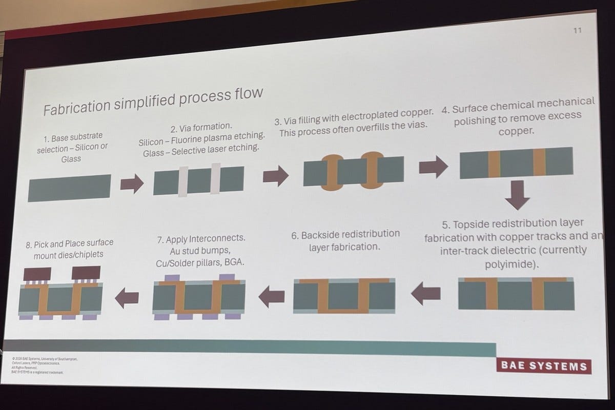
In selective laser etching, a laser weakens the glass along the outline of each via so a chemical bath eats through it thousands of times faster than the surrounding material. The central core then falls out, leaving vias 300 microns deep and 40 microns wide on a 60-micron pitch.
Dies were attached with gold stud bumps (tiny gold balls on a chip's bond pads that can be flipped and bonded face down) and tested for shear strength. Bonds exceeded 25 gram-force per bump, five times the minimum set by the US military standard MIL-STD-883.
“We’re well above the military standard for these kinds of things, and we showed that we can get a nice electrical connection through our interposer and up into our dummy chip and back out,” Butterworth said.
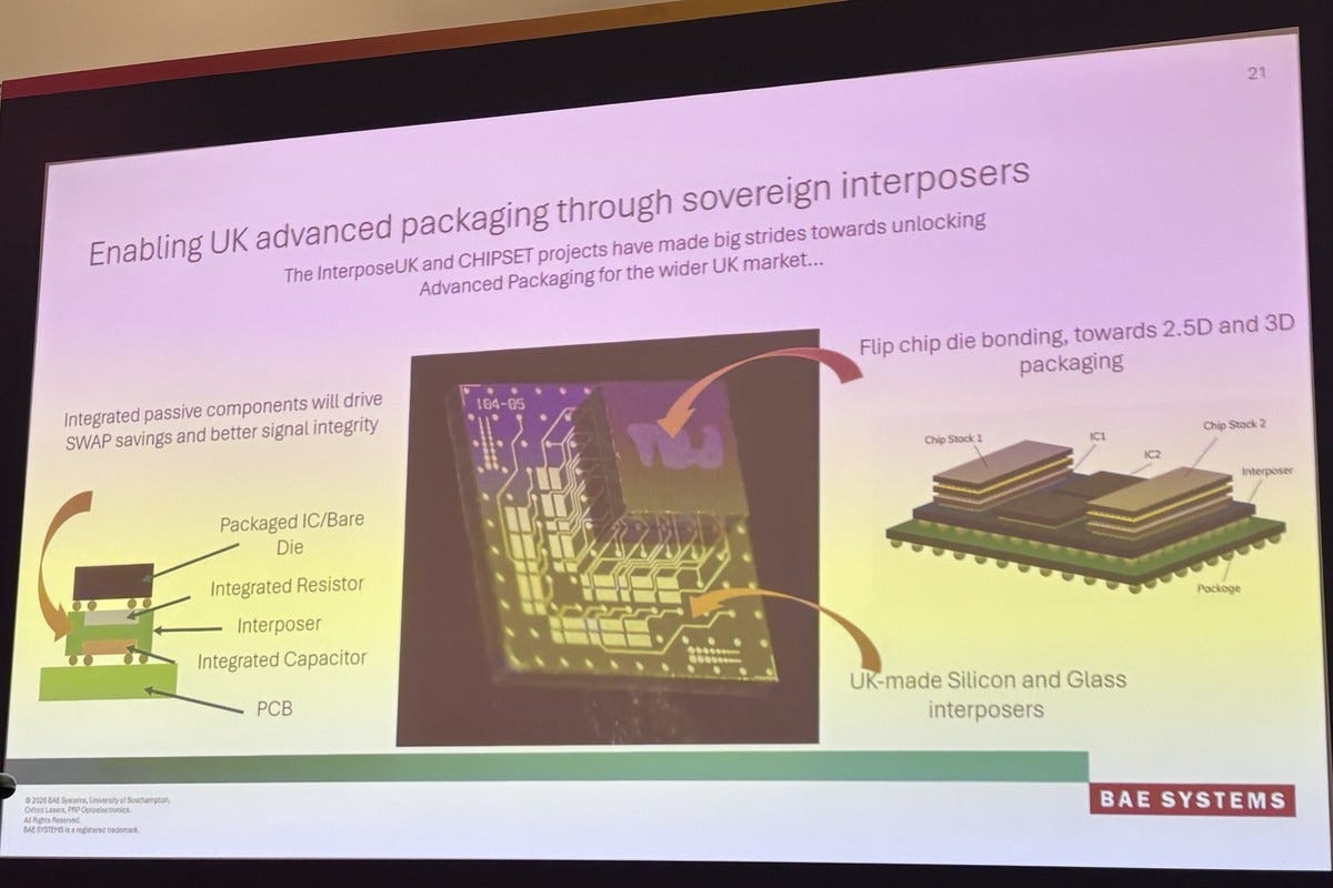
The work came from two Innovate UK projects led by BAE Systems. InterposeUK, which ran from June 2024 to June 2025, produced an initial silicon-and-glass offering. CHIPSET, from October 2025 to March 2026, added passive components and flip-chip bonding.
The partners split the work:
BAE Systems’ FalconWorks unit: silicon vias, design, testing and characterization
University of Southampton: copper electroplating, polishing and redistribution layers
Oxford Lasers: via formation in glass
PRP Optoelectronics, which supplies micro-LED displays for civil and military aircraft: gold stud bumping, flip-chip assembly and testing
The team built its own dummy chips carrying resistors, inductors and capacitors, as sourcing and wiring up a real integrated circuit (IC) would have taken too long in a six-month program.
Months rather than years
Butterworth said simple devices like those in his slides could be made now, though the team still needs more statistical data on its processes.
“In the early stages, there’s going to have to be a reasonable amount of back-and-forth with your design. We’re not talking years away. We’re talking hopefully months away,” he said, answering an audience question on when the interposers would reach the market.
He said the interposer is a generic platform technology, not yet narrowed to one use.
The next gains in size, weight and power (SWaP) could come from building passive components into the interposer instead of mounting them on the circuit board.
“Everyone is space constrained in their platform, so we can save more space by putting more onto that silicon. Rather than these being surface-mount components on a PCB board, we can mount everything vertically and drive down the overall footprint,” Butterworth said.
The team made thin-film nickel-chromium resistors, multilayer thin-film capacitors and planar inductors. Integrating them cuts the number of connections outside the package, saving space and improving security, his slides said.
Trench capacitors offer higher capacitance but need an atomic layer deposition (ALD) tool, which the consortium lacked.
Other gaps lie in the supply chain itself. The team looked at alternatives to gold stud bumping, but importing the chemicals took longer than the project allowed because no one else in the UK uses them, Butterworth said.
“We’re not wed to gold stud bumping, but it’s the easy starting point,” he said.
Copper and solder pillars are in development, and silicon carbide substrates for high-power devices are on the roadmap, though they are far less mature than silicon and glass.
A consortium partner in the audience said selective laser etching can also carve 3D structures inside glass.
“Is this something you want in terms of a sovereign product to drive the next generation of your electronic products? We certainly think so, but we’re biased because we did the work,” Butterworth said.
The consortium has made laboratory-scale demonstrators and is now refining its process to improve yield, while seeking early users to steer what it builds next.